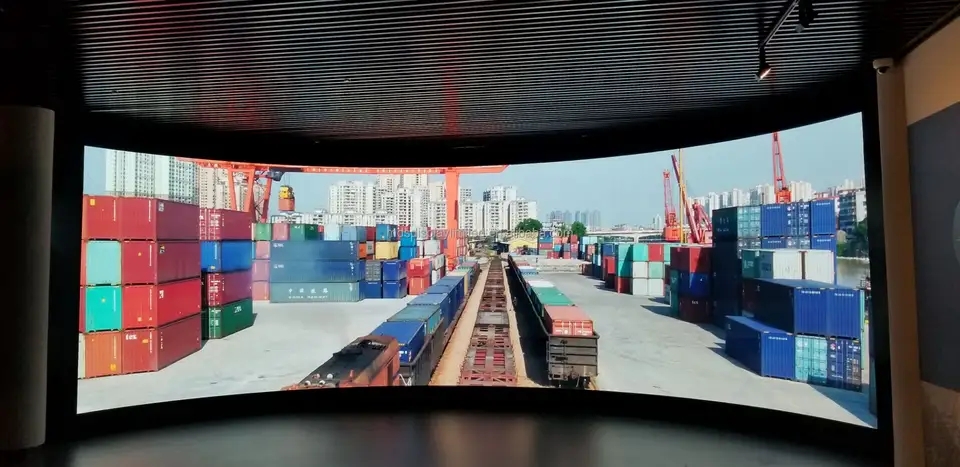
With the rapid progress of LED display technology, the dot spacing of LED screens is becoming smaller and smaller. Now, the market has launched high-density LED screens with P1.4 and P1.2, and they are beginning to be applied in the fields of command and control and video surveillance.
So what issues should high-density LED screens pay attention to? The reason why high-density LED screens have taken the lead and are in huge market demand is because high-density LED screens have characteristics such as high clarity, high refresh rate, seamless splicing, good heat dissipation system, and convenient and flexible disassembly and assembly. With the decreasing pixel spacing, higher requirements are being placed on the installation, assembly, splicing process, and structure of LEDs. Lei Ling Display will explore some process issues:
1. LED selection: Display screens with a density of P2 or higher generally use lights of 1515, 2020, or 3528, and the LED pin shape adopts J or L packaging. When welding the pins laterally, there will be reflection in the welding area, and the ink effect is poor. It is necessary to add a mask to improve contrast. The density further increases, and the packaging of L or J cannot meet the minimum electrical performance spacing requirement, so QFN packaging must be used. Both the 1010 of Guoxing and the 0505 of Jingtai use this packaging.
Unique QFN packaging and welding process, characterized by no lateral welding pins and no reflection in the welding area, resulting in excellent color rendering effect. In addition, it adopts a fully black integrated design and molding, which increases the contrast of the screen by 50%, and the image quality effect of the display application is better than that of previous displays.
2. Process selection for printed circuit boards: With the trend of high density, 4-layer and 6-layer boards will be adopted, and printed circuit boards will adopt micro through hole and buried hole designs. The printed circuit graphic wires will be fine and microporous with narrow spacing, and the mechanical drilling process technology used in processing can no longer meet the requirements. The rapidly developing laser drilling technology will meet the needs of micro hole processing.
3. Printing technology: Excessive or insufficient solder paste and printing offset directly affect the welding quality of high-density display screen tubes. The correct PCB pad design needs to be communicated with the manufacturer and implemented in the design. The size of the screen opening and the correctness of printing parameters directly affect the amount of solder paste printed. Generally, 2020RGB devices use electropolished laser steel mesh with a thickness of 0.1-0.12mm. For devices below 1010RGB, it is recommended to use steel mesh with a thickness of 1.0-0.8. The thickness, opening size, and tin content increase proportionally. The quality of high-density LED welding is closely related to solder paste printing, and the use of printing machines with functions such as thickness detection and SPC analysis will play an important role in reliability.
4. Installation technology: The slight deviation of RGB device positions in high-density display screens will result in uneven display of the screen body, which inevitably requires higher accuracy of the installation equipment. The installation accuracy of Panasonic NPM equipment (QFN ± 0.03mm) will meet the installation requirements of P1.0 or above.
5. Welding process: If the temperature rise of reflow soldering is too fast, it will lead to uneven wetting, which will inevitably cause deviation of the device during the wetting imbalance process. Excessive wind circulation can also cause displacement of the device. Try to choose a reflow soldering machine with a temperature range of 12 or above, and strictly control the chain speed, temperature rise, and circulating wind force as items to meet the reliability requirements of welding while reducing or avoiding device displacement, and try to control it within the required range. Generally, a range of 2% of pixel spacing is used as the control value.